
The PCB (printed circuit board) is at the heart of every electronic circuit. It’s responsible for electrical connections between components and interfacing devices with the world. A small error made during design may cause delays, increase costs of manufacturing, and/or lead to malfunction/failure of the circuit. PCB design engineers need to be aware of and concerned with the complex details of the PCB. The following are the most common mistakes to avoid in PCB design and assembly.
- Incorrect trace geometry: Traces control the transmission of electrical signals between the components of a circuit. They must meet precise constraints of speed, intensity, and frequency of the signal. The geometry (length, width, thickness, spacing) of each trace affects the circuit and must be correct.
- Insufficient layout: The demand for smaller and smaller circuit boards is growing, forcing designers to reduce distances between components and utilize components with small footprints. An inefficient and/or inadequate layout creates a risk of non-compliance and/or connection issues. Designers must select a layout that meets the needs of each particular circuit. It’s wise to allow space on the PCB for alternative and/or additional components to meet possible future needs.
- Poorly positioned decoupling capacitors: Decoupling capacitors ensure a stable power supply that is free from oscillation (a cyclical variation in voltage and/or current resulting in a periodic waveform) and transients (reactions to the variations of driving voltage and/or current). Capacitors need to be closely placed to the component pins and connected parallel to the power supply.
- Errors in the landing pattern: A landing pattern is determined by the size of the pads utilized for each component and should be slightly larger than the corresponding component footprint. Errors in spacing cause problems during the manufacturing process resulting in misalignments between the PCB and components. If the distance between pads is incorrect, the pins will not align making soldering difficult and/or impossible.
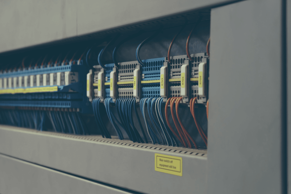
- Overuse of automatic routing results in via holes that are larger than those accomplished when using manual routing, occupying more area of the printed circuit board and affecting the manufacturing cost for the PCB.
- Sizing and type of vias: Via holes enable the solving of many complicated routing issues and improve the heat exchange of the PCB. Blind vias connect an internal layer to an external layer. Buried vias are used to connect 2 internal layers. Through-hole vias connect two external layers and sometimes internal layers. Blind and buried vias are more costly to produce and often need to be kept to a minimum to meet the budget allocated. Inexperienced designers often make the drill diameter of vias too large or too small, to be reliably manufactured.
- Electromagnetic interference may be caused by inappropriate design of the PCB. To avoid this issue, group elements by functionality (power section, analog block, digital block, high-speed circuits, low-speed circuits). Use metal containers to shield cables and reduce or eliminate right angles on the traces.
- Incorrect antenna layout: If the PCB contains antennas for wireless communication, adapt the impedance between the antenna and the transceiver. Use a Pi (LC) tuner filter between the transceiver and the antenna for accurate impedance adjustment.
- Insufficient design review: Design review is a crucial step in PCB development. A peer review by a team member allows for verification of high-level requirements, the assigned functions, and interconnection between circuits, enabling designers to detect/avoid common errors.
- Decoupling: Correct decoupling is crucial to a well-functioning, stable system ensuring power delivery to integrated circuits requiring high power for a short time. Place decoupling capacitors close to relevant integrated circuit pins, use short and wide traces, and place power vias close to each other.
- Reference planes: Electricity/signals travel in closed loops that require a return to the source. Use solid references when designing (OV or GND planes). Ensure that AC signals have a reference plane below and avoid creating large voids/splits in this plane. Do not cross splits with a signal layer or a trace.
- Failure to make a backup: Software and data are used to achieve good results when designing a PCB. Data can be lost due to the high flexibility and speed of the software. Create save points and save your data often.
- Lack of Communication: Miscommunication due to stress, fatigue, and multitasking leads to increased cost and added operation time. Proper communication can assist in meeting the promised delivery date.
Many common mistakes occur during the process of designing a PCB, increasing the cost of production and often resulting in a flawed prototype. The above information can assist designers in creating a successful PCB quickly and economically.
Looking for an affordable, cost-effective PCB design and assembly? Our Calgary-based team of dedicated, skilled, knowledgeable people offers unparalleled products and services. Innovative Manufacturing Source (IMS) helps you through in-house manufacturing completed on state-of-the-art equipment/tools. Call 403.279.7702 and allow us to be your provider of custom metal fabrication services and electronic manufacturing. We support customer-specific requirements on everything that we produce.